Warehouse Challenges for Semiconductors

Industry challenges
»
Global demand - The multi-fold growth in demand for semiconductors due to the increase in data centres, led by Generative AI, has led to manufacturing facilities operating at maximum capacity. Any bottlenecks on production lines or inventory movement can result in unexpected delays.
»
Handling Ultra Sensitive & Fragile Components - Wafers used to make chips, are very thin and brittle. Small vibration or dust can lead to irreversible damages, resulting into batch losses.
»
Environmental Control & Monitoring - Semiconductor chip fabrication requires tightly controlled cleanrooms maintained at strict humidity, airflow, and temperature levels, especially for Moisture Sensitive devices (MSDs). Manual handling poses the risk of particle intrusion, risking production quality.
»
Safe Transport Between Cleanroom Zones - It is a best practice to do materials movement across zones with varying cleanliness grades without human intervention to avoid contamination.
Industry challenges
»
Lot-Level Traceability & Error-Free Inventory - Each lot of ICs are made with expensive raw materials. Batch mix-ups of any raw material due to age, quality or availability can cause immense financial losses and production shutdown.
»
High Security Against Counterfeit & Theft - The semiconductor manufacturing process produces high-value chips that are small, lightweight, and easy to steal. Weak warehouse controls increase risks of counterfeiting, IP leakage, and black-market diversion.
»
Electrostatic Discharge (ESD) - Humans and mechanical equipment can develop static electricity; ICs are extremely sensitive to ESDs which can cause irreversible damage.

Automation Solutions for Semiconductor

Controlled Storage

Collaborative robots

Precision Movement

AI enabled Software

Secure production

Compliant Solutions

Slide Image

Our specialized ASRS for semiconductor industry - Vertix, offers dense storage, faster retrieval, and accurate order picking of reels in dirt-free cleanroom conditions, without safety compromises. Our robots are ISO and ESD compliant, ensuring highly reliable and scalable implementation of new production lines as per demand.

Slide Image

Automated robotic picking systems handle front open unified Pods (FOUPs) with smoothness and accuracy. This ensures safe handling of fragile semiconductor parts while supporting buffer supply to fabrication lines and assembly processes.

Slide Image

Our mobile manipulator robot which is an AMR robot combined with a sensitive pick and place arm assures accurate and contamination-free lot movement of chips & wafers. With a cleanroom compliant design, it provides a safe environment for both humans and robots.

Slide Image

Our Advanced AI enabled software suite provides real-time trace of silicon wafers, FOUPs in production stage and seamless integration with MES (Manufacturing Execution System), further boosting production speed and order accuracy.

Slide Image

Addverb software suite comes with user level access restrictions, digital logging, and intelligent tracking that protects high-value semiconductor chips. This prevents risks of theft, leakage, or counterfeit entry while maintaining integrity and trust across the supply chain.

Slide Image

Our robots are designed to be safe and compliant with strict control parameters, meeting high quality standards. This makes them suitable for integration with many cleanroom applications for handling of highly sensitive microelectronic devices.

Solutions Finder

Your biggest challenge?
Gran número y variedad de SKU
Manipulación frágil de los productos
Requisitos medioambientales de los productos
Visibilidad inadecuada del inventario
Inexactitudes e ineficiencias en el picking y la clasificación

Descargue nuestro folleto

Descargar

¿Busca una solución?

Póngase en contacto con nosotros

Automatización eficiente para la industria de semiconductores

¿Por qué elegir Addverb?

Automatización para la industria

Una industria que se enfrenta a rápidos cambios tecnológicos necesita una solución de automatización que pueda adaptarse rápidamente. Lea nuestro estudio de caso para conocer las soluciones innovadoras que ofrece Addverb.

...
Blog destacado
Almacenamiento de semiconductores: Retos, soluciones y automatización

Alrededor del 25 % de los almacenes de todo el mundo habrán adoptado algún tipo de automatización en 2024. Sin embargo, solo el 10 % utiliza la automatización avanzada de operaciones. Lea el blog para desentrañar varios retos clave en semicon...

Productos para semiconductores

Nuestra amplia cartera de productos nos ayuda a diseñar soluciones personalizadas para los distintos requisitos del sector.

Otras industrias

Preguntas frecuentes

  • What factors determine the cost of automating a semiconductor warehouse or cleanroom?

    The cost depends on the required automation modules, contamination control level (ISO class) and type of automated transport systems (like AMRs, FOUP/FOSB storage). Since semiconductor operations have stringent ESD and cleanliness requirements, solutions are highly customized. For an exact cost estimate, please get in touch with our experts here.

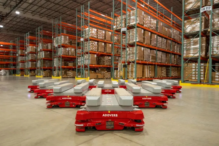
  • How long does it take to implement automation in a semiconductor environment?

    Implementation timelines depend on cleanroom layout, throughput required, and integration with existing MES and fab systems. Modular solutions such as FOUP transport Mobico or automated Vertex can go live in phases within months. Stepwise deployment ensures zero contamination risk and seamless handover across cleanroom zones.

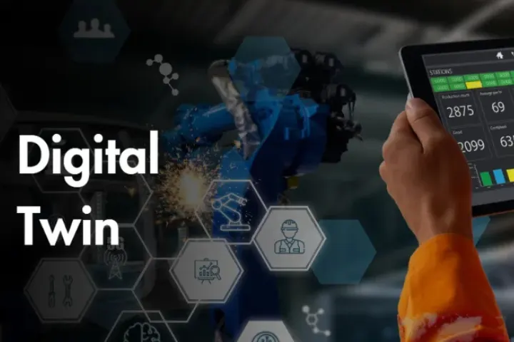
  • How can digital twin simulation help optimize semiconductor logistics?

    Addverb’s digital twin models wafer flows, FOUP transfers, and buffer storage under varying throughput scenarios. This helps fabs test layout efficiency, predict bottlenecks, and validate system capacity before deployment, reducing commissioning time and ensuring flawless integration with fab operations.

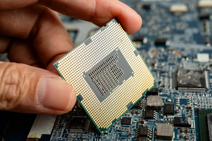
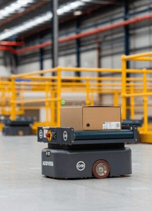
  • How do Addverb’s solutions ensure contamination-free and ESD-safe handling?

    All our cleanroom AMRs and robotic systems use anti ESD materials and have smooth movement for handling fragile components of semiconductor production. Integrated sensors monitor particle count and ESD parameters in real time, ensuring contamination-free transport of wafers, and critical components.

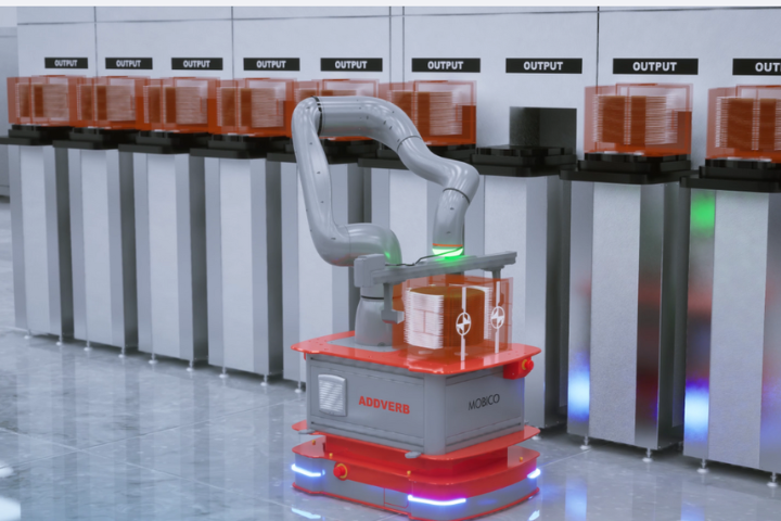
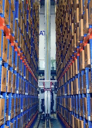
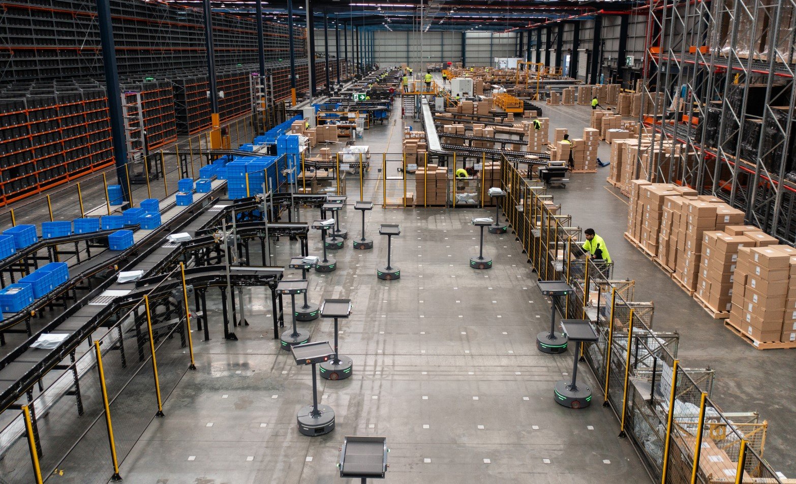
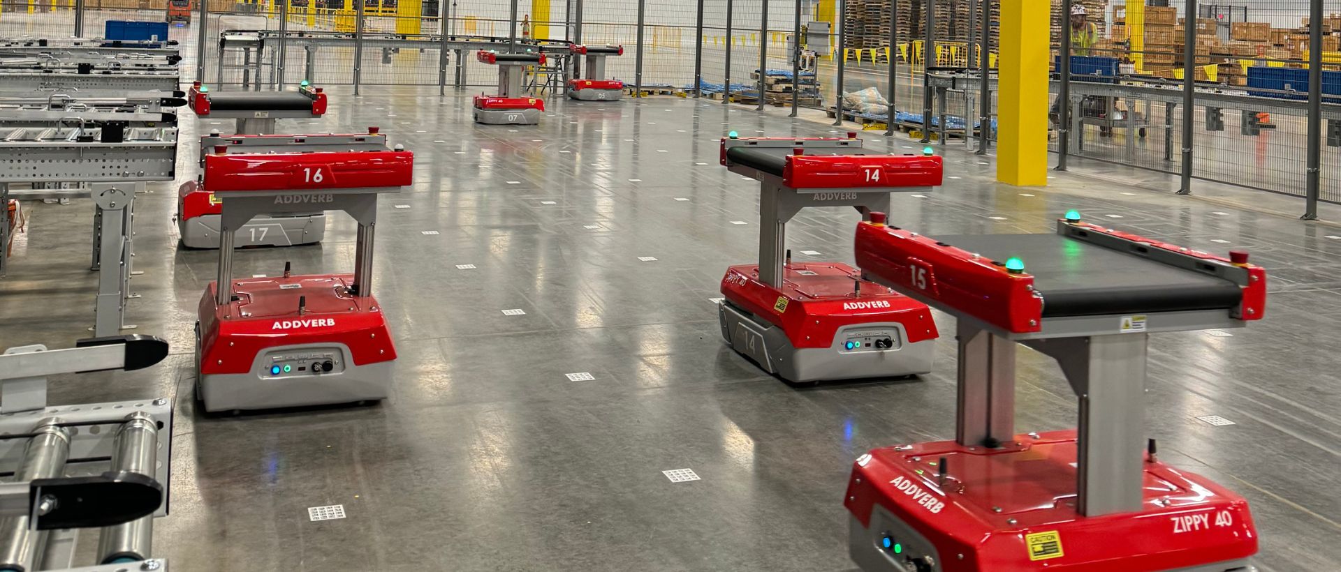
  • Can Addverb automation scale with fab expansion or new process lines?

    Yes. Our modular automation like FOUP transfer AMRs, Wafer disk ASRS can be easily scaled or reconfigured as new bays, or process lines are added. Our Seamless software integration ensures synchronized wafer flow and real-time updates across MES and warehouse control systems.